
Custom printed circuit boards, manufactured in Brazil since 1986
Micropress is a Brazilian printed circuit board (PCB) manufacturer. We produce double-sided and multilayer boards, from prototypes to series production, in our own factory in São Paulo, with engineering support from the review of your files onwards.
Request a quote Chat on WhatsApp
- 1986manufacturing PCBs in São Paulo
- Up to 24 layersmultilayer, on request
- 0.10 mmminimum track width and spacing (4 mil), with 1 oz finished copper
- IPC Classes 2, 3 and 3/Aper IPC-6012 and IPC-A-600
What we manufacture
We build to the customer's design: every board is produced from your manufacturing files and your specification.

Double-sided PCBs
Two-layer boards with plated through-holes, in FR-4. We also make single-sided boards in FR-1 (1.6 mm thick) and in FR-4.
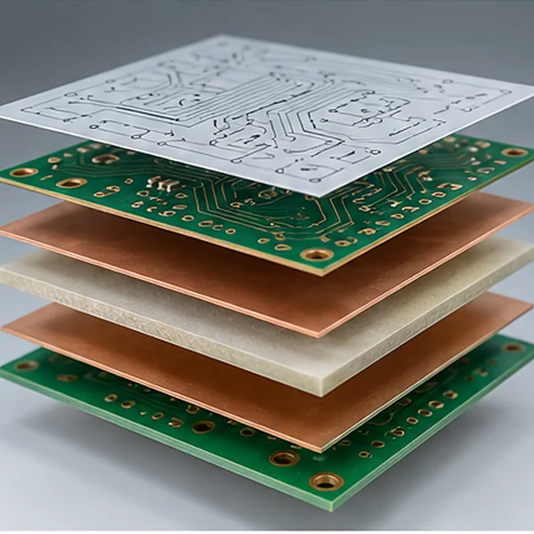
Multilayer PCBs
From 3 to 24 layers, on request. Blind and buried vias are produced subject to technical review.

Metal core (MCPCB)
Metal-based boards, 1.5 mm thick, for applications that require heat dissipation.
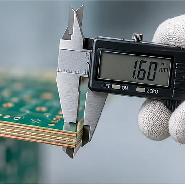
From prototypes to series production
We handle prototypes, small batches and series production. The feasibility of each order is confirmed against our standard capabilities.
Standard capabilities
Key manufacturing limits. The complete values, item by item, are on the technical capabilities page.
| Materials | FR-1 (single-sided, 1.6 mm), FR-4 (single-sided, double-sided and multilayer) and MCPCB (metal core, 1.5 mm); Tg 140, other Tg values on request; materials subject to availability |
|---|---|
| Layers | Single-sided, double-sided and multilayer from 3 to 24 layers, on request |
| Finished board thickness | 0.8 to 3.2 mm (±10%) |
| Base copper | 17, 35 and 70 µm (½, 1 and 2 oz) |
| Minimum track width and spacing | 0.10 mm (4 mil) with 1 oz finished copper on outer layers |
| Minimum plated hole | 0.15 mm (6 mil) in FR-4 up to 1.6 mm; maximum aspect ratio 10:1 |
| Blind and buried vias | Subject to technical review |
| Solder mask | Green, red, blue, black, white and clear |
| Surface finishes | HAL Sn/Pb (hot air levelling), OSP, ENIG (electroless nickel immersion gold) and solderable varnish |
| Additional finishes | Electrolytic gold flash on contacts, carbon and peelable mask; IPC-6012 compliance for the gold on request only |
| Maximum board size | Up to 420 × 570 mm for boards without electrical test and without V-scoring; with electrical test or V-scoring, the maximum size is smaller; MCPCB on request |
| Accepted files | Gerber RS-274X, Gerber X2 or ODB++, compressed in a ZIP file |
| Acceptance | IPC-6012 and IPC-A-600, Classes 2, 3 and 3/A |
Source: CP document — Standard Technical Capabilities, revision 19, dated 30 October 2025. Features outside this standard are accepted only after prior review and approval.
How it works
Send your files
Gerber RS-274X, Gerber X2 or ODB++ in a ZIP file, with quantity, layer count, thickness, copper, solder mask colour and finish.
Technical review
Our technical support reviews the files and the specification against our manufacturing capabilities.
Quotation
We send you a quote with price, manufacturing lead time and shipping conditions.
Manufacturing and shipping
We manufacture in São Paulo, with inspection and electrical testing according to the order specification, and ship under the agreed terms.
Why Micropress
Our own factory
Your board is manufactured in our São Paulo plant, where we have been producing printed circuits since 1986.
Engineering support
Technical support from the review of your Gerber files through to electrical testing.
IPC acceptance criteria
Performance and acceptability requirements per IPC-6012 and IPC-A-600, Classes 2, 3 and 3/A.
Published capabilities
Our manufacturing limits are published item by item, so you can check your design before requesting a quote.
Current processes
Laser direct imaging (LDI) and HAL, OSP and ENIG finishes, among others.
Open technical knowledge
We publish the Professional PCB Guide, a 19-chapter guide to board manufacturing and specification (in Portuguese).
Orders from outside Brazil
- Each international quote states the currency, payment terms, manufacturing lead time and shipping method.
- Taxes, import duties, customs clearance and any other charges in the destination country are the buyer's responsibility, unless expressly agreed otherwise in the commercial terms.
- Manufacturing depends on technical approval of the files. Features outside our standard capabilities are accepted only after prior review and approval.
- The full technical documentation on this website is in Portuguese.
Request a quote
Fill in the form and attach your manufacturing files. We will reply by e-mail.
Other channels
- +55 11 2940-6262
- comercial@micropress.com.br
- Address
- Rua Angaturama, 51 – Vila Moraes
São Paulo – SP, 04164-010
Brazil
Brazil time (UTC−3).